Physical memory security vs. virtual memory security
While developing our mobile hardware models, we've run into a large array of schemes aimed at improving physical memory security. The sheer ingenuity displayed by the engineers in coming up with them often goes unnoticed, even by technically inclined users, because most of the time these mechanisms are quietly working in the background acting as mitigations for potential complex exploit chains.
Instruction-level schemes that focus on hardening virtual memory access of one kind or another (code flow, heap allocation) have been receiving a lot of attention, for instance ARMv8.3-PAC or ARMv8.5-MTE. They are aimed at solving different problems so we won't talk about them here.
So let's talk about the physical ones.
1. What is physical memory security?
Modern mobile devices have grown in complexity at a breathtaking pace. A classic GSM mobile terminal with GPRS would probably include a single core, perhaps an ARM7 or ARM9, a modem handling most of the core functionality, and a simple text-based AT command protocol running between those two. The physical RAM of the Application Processor (AP) would be really quite private to it, with little in the way of DMA, and no way to access it from other programmable processors.
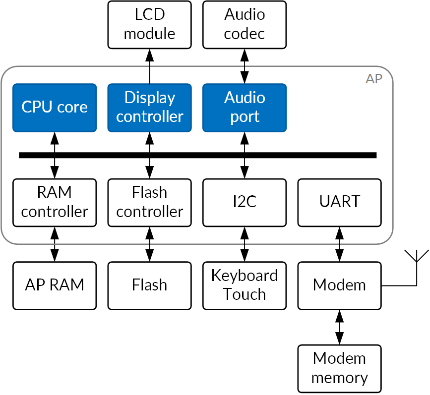
Fig.1: A classic mobile terminal
This is as far from a modern smartphone as you can imagine.
A typical smartphone SoC in 2020 includes multiple requesters sharing the address space - not just many cores in the AP, but also multiple, possibly heterogeneous, cores running key functions such as digital signal processing for modem, audio and camera, 3D graphics hardware, (overly) flexible DMA blocks, low-power-mode system control processors, and others. The cores that can perform main memory operations number in tens now. For instance, the Apple A14 includes no fewer than 12 "accessory" ARM cores in addition to the 6 visible to the user software, two audio DMA controllers, three graphics support blocks (all with DMA capability) and an encryption block. Even older parts such as the Qualcomm Snapdragon 845 will have upwards of ten memory requesters.
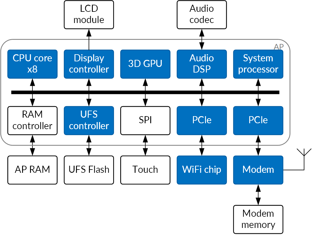
Fig.2: A modern smartphone
Arbitrary, unrestricted memory access by any single one of these cores can lead to a complete compromise of the SoC. Their heterogeneous nature means each of them can have its own set of security vulnerabilities. It's hard enough to write reasonably bug-free software once; doing it multiple times makes it exponentially harder.
In addition, there are now paths in the system that allow the injection of memory access commands from the outside. The most notorious one of these is PCI Express, which is designed for efficiently performing memory accesses to the host's memory. But a poorly secured debug path into any of the other cores can also result in memory access injection.
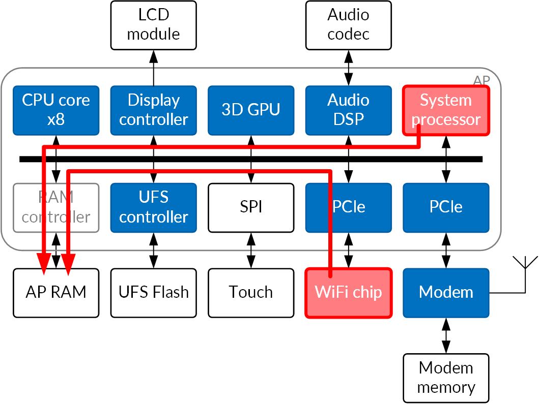
Fig.3: Attack paths in a modern smartphone (PCIe, compromised coprocessor)
2. ARM architecture can help solve physical memory security issues
The lowest-cost solution to some of the issues with physical memory security is to use a higher privilege level in the main CPU core to control DMA configurations of other blocks or provide security to access from the CPU itself.
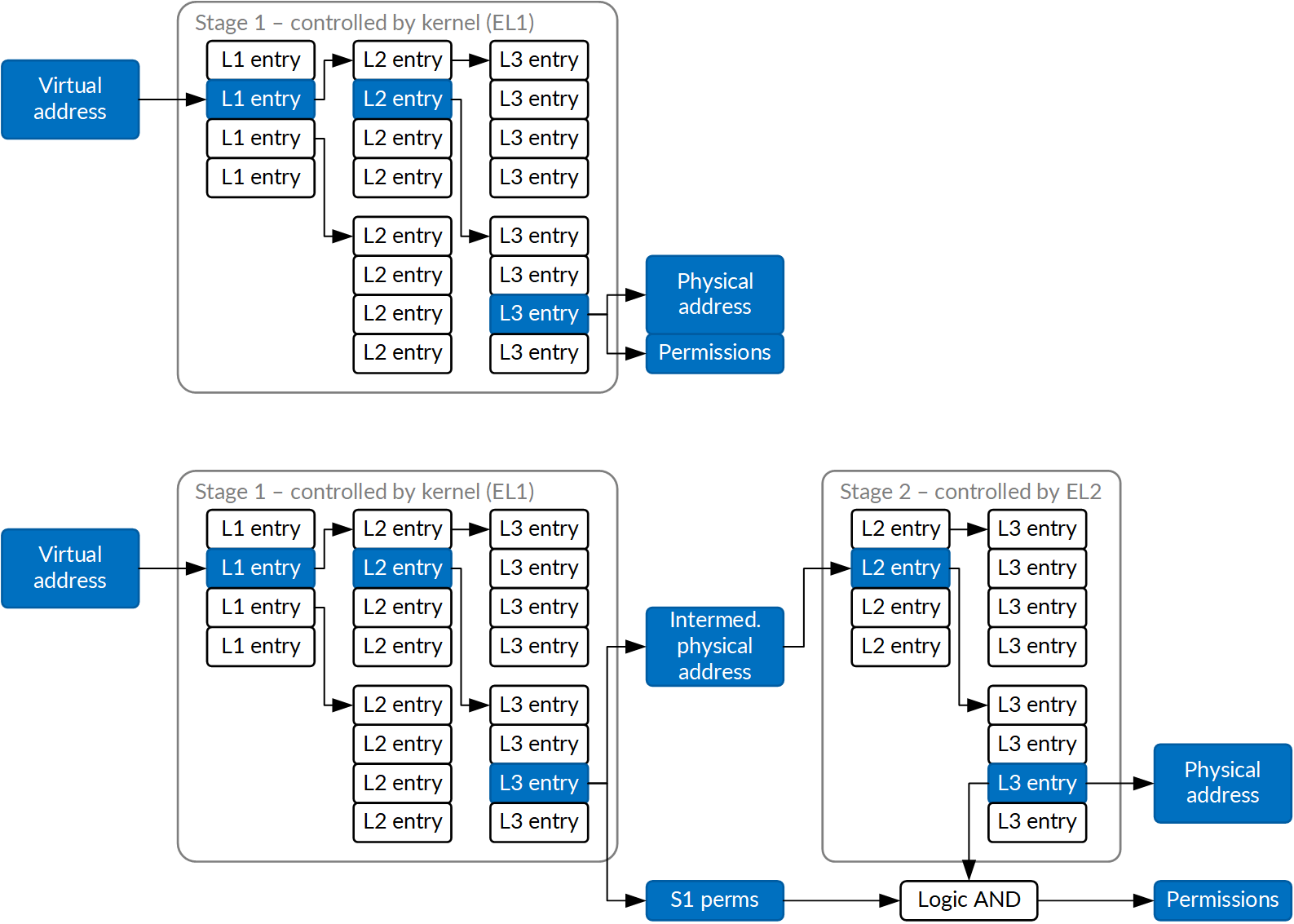
The ARM architecture provides a mode perfectly suited to this task. The EL2 mode, intended for accelerated hypervisors, has seen significant use on both Samsung and Huawei devices as a security-privileged execution mode instead. It can restrict access to physical memory and memory-mapped I/O using second-stage memory translation, and from that primitive a pretty compelling security architecture may be constructed.
Let's start with an example of a simple DMA block that moves data from system memory to an I/O device, or perhaps another place in memory.
Typically, DMA configuration is set by a driver running in the operating system kernel, so in EL1 in modern ARM privilege level hierarchy. A lot of the configuration will be fairly non-sensitive: endianness translation, timestamps, element and FIFO sizes being set incorrectly would be perhaps disappointing or unpleasant to the user - especially in the case of audio, as anyone who ever worked with audio DSP will certainly appreciate - but not really leading to the system compromise.
There are in fact only two key elements to a DMA transfer configuration that really matter from a security standpoint: base address and transfer size. So, some hardware vendors have these two registers filled out by software running at a higher privilege level. That software can vet the physical memory address passed to it and make sure the configuration written to the hardware will not violate security assumptions of the system. All that's required to make this a pretty good approach is to make those registers non-writable by ordinary kernel code, for instance by putting them in their own page-sized memory range, and using second translation stage (controlled by EL2 privilege level) to prevent EL1 (kernel) access.
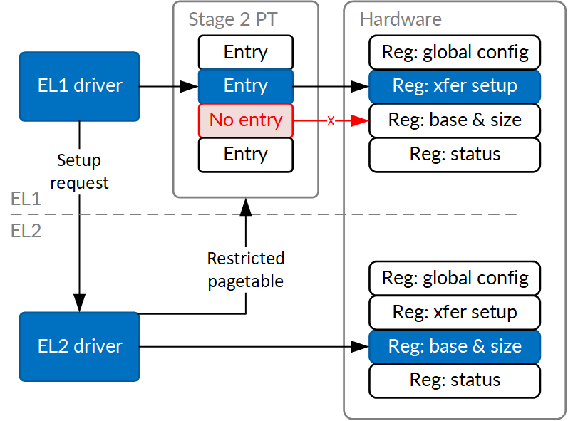
This approach works really well for simple DMA controllers, where vetting the address/size block pairs is sufficient. It does not work as well for mitigating compromises caused by fully programmable accessory processors, but it's still a valuable component of other mitigations - for instance by ensuring the kernel cannot surreptitiously disable them without going through validation at a higher privilege level.
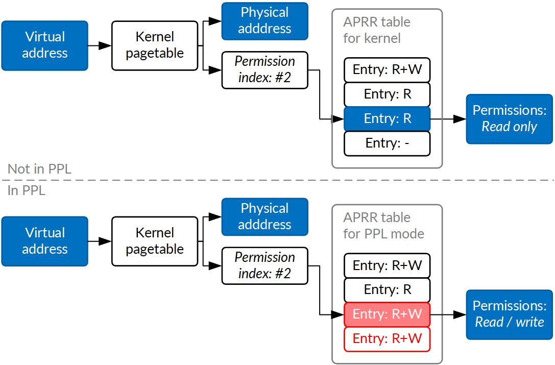
Additionally, once built, the same mechanism can be used to protect other system security guarantees. For instance, Samsung and Huawei devices use EL2 to protect pagetables and some security-critical kernel structures (SELinux, credentials and similar); writes to pagetables must go through EL2, which makes sure the kernel does not attempt to map memory or MMIO that it has no right to use. Similarly, Apple processors modify their understanding of memory page permission bits when they run a special, separate piece of code responsible for pagetable modification (PPL) using a novel mechanism called APRRs. In this case, EL2 is not used, but on newer SoCs, a "lateral" exception level has been introduced with much the same effect on access permissions.
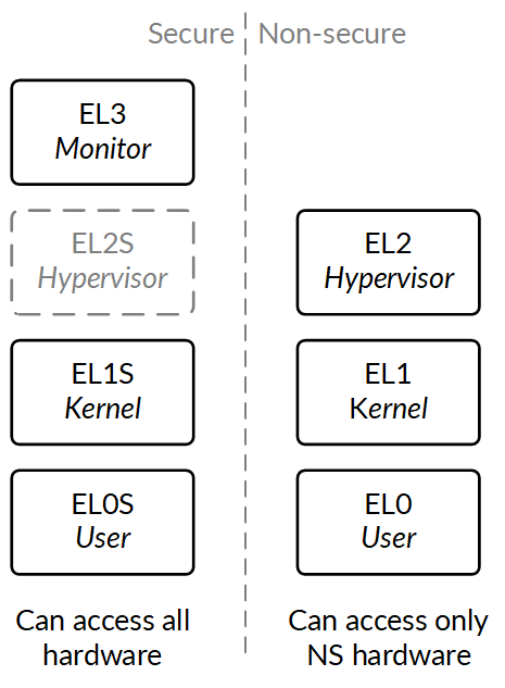
Lastly, any discussion of elevated protection levels must necessarily include ARM architecture's Secure mode. This long-standing feature of ARM processors, included in the TrustZone feature set, allows the processor to run in two "worlds": secure (S) or non-secure (NS). Most regular operating system software would run in NS world (EL0NS to EL2NS), but critical security functions could run in EL0S or EL1S.
What makes this mode different from the EL2, APRR or "lateral" exception level based security is the concept of marking every memory access request with the world it came from. Then, memory controllers and peripherals can decide to accept (or not) NS requests. There's a cost to making that work well: caches need to retain information on the world each cacheline is meant for. However, it's also a more powerful mechanism for DMA protection: DMA controllers and accessory processor requests could also be classified as S or NS, and their memory accesses could be subject to the same restrictions.
In many ways, this is the prototypical hardware physical memory security solution, pioneered by the Broadcom secure application processor line, and extended into many refined versions giving more fine-grained control. Time to talk about these.
3. Memory security methods for address filters
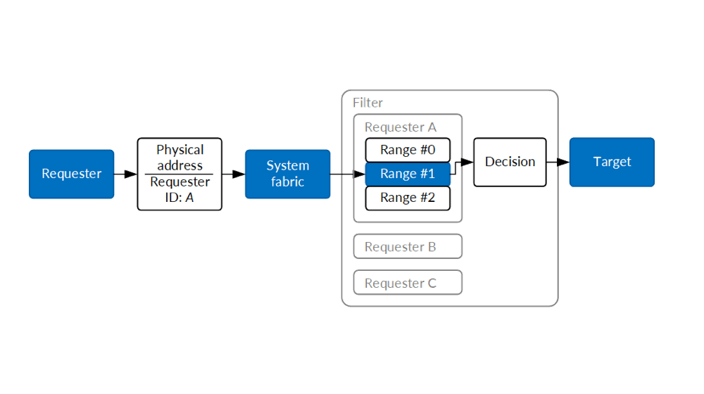
The tags on memory requests can be extended beyond Secure / Non-Secure. For instance, they can include the requester's identity: did the request come from the AP, or from the audio DMA controller? Some requesters can be even more flexible, including a "stream ID" with their request: is this request retrieving a next DMA descriptor (which contains physical addresses, and can lead to compromise) or just audio data (which does not)? This is the foundation of a whole family of physical memory security methods, the first of which - and the simplest - is the address filter.
Sometimes, all that's needed is to give a specific DMA block (or processor) permission to access the memory range. There are two common approaches to this. One can insert a hardware block between the DMA block and the system fabric (which routes memory requests around the SoC) and have it compare addresses on the outgoing requests against a list of ranges, perhaps configured by MMIO from the main system processor (running in a higher privilege mode, to protect it better). Only requests that hit one of these specified ranges will be allowed to proceed to the system fabric for fulfillment. This is how the DAPF block works on Apple CPUs.
Other approach is to put the enforcement on the target side of the request. Target side enforcement requires the system fabric to route the security tag from the source, and to make sure that the "requester identity" part of the security tag is in line with the actual requester; after all, if a programmable requester could freely spoof the tag on the bus, that is to claim the request originated from someone with higher privileges, the system security guarantees may not be met.
This approach is used by the original Secure / Non-Secure peripheral classification in TrustZone ("only Secure requesters may touch this peripheral") and dedicated memory ranges for accessory processors ("only modem DSP can use this range of memory, because it's its own program / data memory"); those would be enforced at the memory controller with a permission bit or range map.
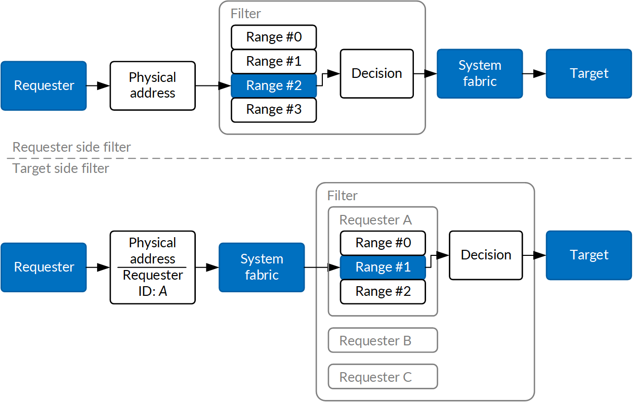
A simplified case would be one where a memory range is fully locked out for write transactions, where the security tag is implicit in access type (is it a read or write?) and the memory controller will deny writes in a list of protected ranges. This is what the AMCC does to protect kernel memory from writes on modern Apple SoCs.
4. An advanced approach for physical memory security: IOMMUs
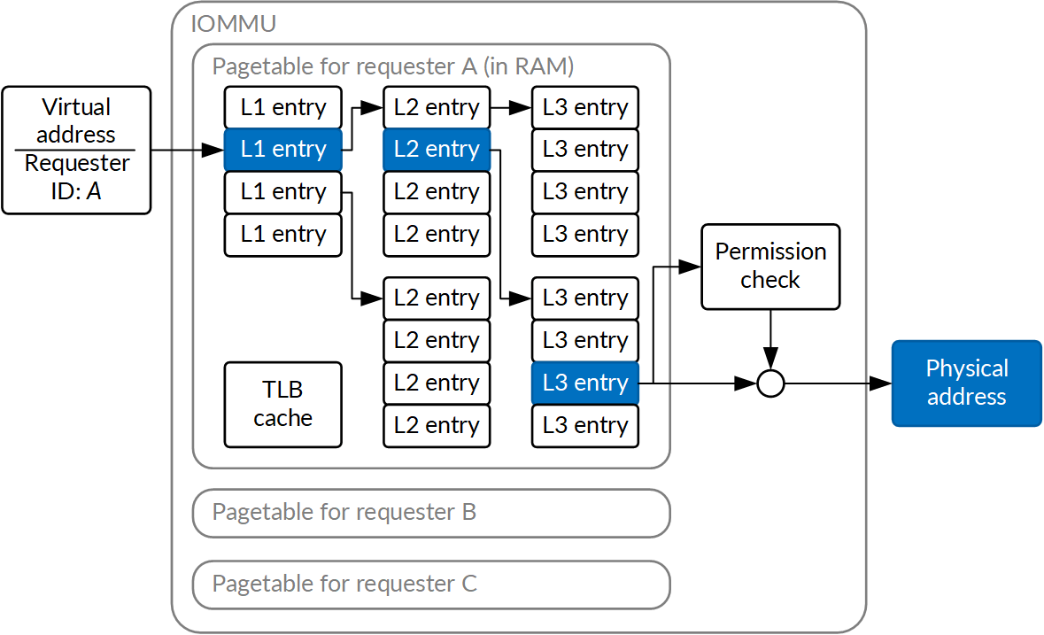
A more advanced and flexible approach to the same problem is called IOMMUs. This stands for I/O Memory Management Units; they create a virtual address space for devices analogous to the virtual addressing in processors. Now, the protection hardware can apply and modify not only permissions, but also the address being accessed. This requires significantly more memory to store the translation and permission map, and usually ends up with a set of I/O pagetables located in memory that the IOMMU reads from as it translates I/O accesses to the target. It's a significant complication compared to using an address filter, where the filter usually fits in the hardware MMIO registers or on-chip RAM visible via MMIO.
What makes IOMMUs so great and worth this effort, however, is their ability to hide physical memory addresses from peripheral devices. This has twofold consequences. From the security standpoint, it means the system memory map is not disclosed to the potentially compromised accessory processor or DMA requester. Additionally, it means non-linearly allocated memory can be presented to the peripheral as a linear virtual address space. This is not only a performance improvement but also massively simplifies DMA requester design and removes the need to program scatter-gather lists into the requester.
While ARM has been promoting the use of centralized IOMMUs with their SMMU (System MMU) specification, Apple SoCs use a different approach. Many of their peripheral blocks have a device called a DART in front of them. But both of those IOMMUs share a general design, which is that each request stream uses a specific pagetable, which the IOMMU walks. The walk results (translations and permissions for a given address page) are cached in a TLB (Translation Lookaside Buffer) local to the IOMMU, which needs to be flushed (discarded) when the pagetables are modified.
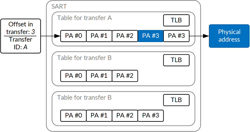
Another, more specialized, kind of IOMMU has shown up in Apple's A10. The NVMe access is performed as fairly long linear transfers, and there's rarely a need to reuse a translation after the transfer is done. So the TLB concept, where all translations share a cache, and are flushed together when any of them is no longer needed, fits poorly. The hardware designers decided to provide scatter-gather tables for each transfer instead; a simple list of target page addresses that a specific range of source addresses would translate to, and make it possible to flush only a single transfer after it's done. This is the SART, and it represents a good example of a custom design guided by performance considerations.
Either way, the task of filling out and managing IOMMU configuration is absolutely critical to security. Otherwise, a perfectly innocuous transfer could instead write arbitrary physical memory, for instance credentials or other permission bits. All of this configuration should therefore be performed by software running at a higher privilege level; this is indeed the case on both Samsung devices with Qualcomm CPUs, and on Apple hardware. They both make it impossible to access IOMMU from lower privilege levels; in the Apple case, by controlling kernel pagetables (which themselves are protected by the APRRs) and in the Samsung case, by second-stage memory translation which is only accessible by EL2.
As a side note, not everyone uses IOMMUs to their full potential. Certain devices use them as a simple address filter, by providing a map of identity address translations and only changing the permission bits. This slightly decreases their utility, but they are still good security.
5. Using memory encryption for memory security
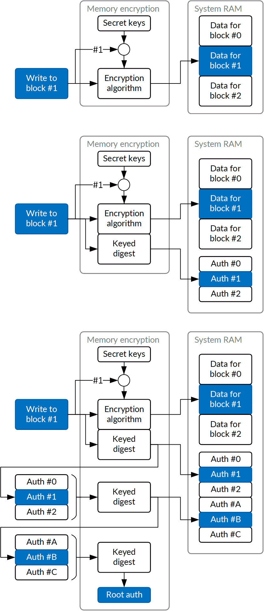
If the attack model is extended to include sophisticated external attacks that include monitoring memory bus transactions, none of these methods are sufficient. After all, if the attacker can directly alter physical memory contents, checking permissions and translating addresses will amount to nothing. If this is a serious consideration, however, a solution presents itself in form of in-line memory encryption.
The simplest form of memory encryption, used for instance on older Freescale (now NXP) devices, would pass the memory transactions through a cryptographic block with a secret key. Let's consider the consequences:
-
memory is now not readable by attackers,
-
path to tamper resistance is easier: just erase the on-chip key when a tamper event happens,
-
as long as the encryption key is derived partially from the memory address, copying attacks are not possible (where encrypted data is moved from one memory location to another in knowledge that it will decrypt to the same plain-text data),
-
corruption attacks are possible, though poorly controllable (a given corruption of encrypted data can produce arbitrary corruption of plain-text data - but sometimes this is a good attack, for instance if software rejects nonsense data or has a faulty error handler!),
-
replay attacks are possible, because there's no way to detect that a memory block was reverted to a previous state,
-
no extra memory or bandwidth is consumed as data does not change size during encryption,
-
latency is low if decryption is started with the requested address.
The corruption and replay attacks are pretty serious. Two subsequent solutions have been deployed to prevent these. The corruption attack can be defended against by adding authentication; a cryptographic keyed digest of a memory block is stored along with it. This solution increases complexity (a digest generator is now needed in hardware, even if it's just AES-GCM authentication tags), memory usage and bandwidth (because authentication data must now be stored) and latency (because the whole block must now be read to verify its digest). This solution is commonly employed, including on Broadcom's pioneering line of secure processors, and likely Apple SEP hardware.
Finally, the replay attack, the hardest one to control, can be prevented by creating a Merkle-tree like structure, in which hashes of lower level blocks (or at least counters used as part of authentication digest key) are themselves authenticated - by storing them in authenticated memory. This creates a multi-level structure, the top level of which will be a single digest authenticating the complete state of all encrypted memory in the system. If that digest is then stored inside the SoC, the externally-initiated reply can no longer threaten the security model. Obviously, the latency cost and complexity get worse, though.
As a side note, memory encryption, even in its simplest incarnation, has a surprising benefit. It practically eliminates electromagnetic emissions from the memory system. In fact, scrambling schemes without cryptographic value have been included in multiple systems expressly for that purpose; but in the context of security, getting rid of compromising emanations may well be worth the effort.
6. End notes
We hope that the security researchers that read our article will recognize these design patterns in systems they encounter; awareness of them means less time spent rediscovering the wheel. At the same time, we hope every hardware designer understands why physical memory security is a key element of a good advanced mobile app security testing strategy, and takes the time to weigh its obvious costs against its numerous benefits; software is never as secure as we hope it would be, and sometimes your hardware is the last line of defense.
Thank you for reading.